- 您现在的位置:买卖IC网 > Sheet目录2040 > PI74ALVCH162601A (Pericom)IC UNIV BUS TXRX 18BIT 56TSSOP
PI74ALVCH162601
18-BIT UNIVERSAL BUS TRANSCEIVER
2
PS8093E 05/23/06
12345678901234567890123456789012123456789012345678901234567890121234567890123456789012345678901212345678901234567890123456789012123456789012
PinName
Description
CLKEN
Clock Enable Input (Active LOW)
OE
Output Enable Input (Active LOW)
LE
Latch Enable (Active HIGH)
CLK
Clock Input (Active HIGH)
Ax
Data I/O
Bx
Data I/O
GND
Ground
VCC
Power
1
2
3
4
5
6
7
8
9
10
11
12
13
14
15
16
17
18
19
20
21
22
23
24
56
55
54
53
52
51
50
49
48
47
46
45
44
43
42
41
40
39
38
37
36
35
34
33
25
26
27
28
32
31
30
29
ProductPinDescription
TruthTable(1,2)
Notes:
1. H = High Signal Level
L = Low Signal Level
Z = High Impedance
↑=LOW-to-HIGHTransition
2. A-to-B data flow is shown: B-to-A flow is similar but
uses OEBA, LEBA, CLKBA, and CLKENBA.
3. Output level before the indicated steady-state input
conditions were established.
4. Output level before the indicated steady-state input
conditions were established, provided that CLKAB is
LOW before LEAB goes LOW.
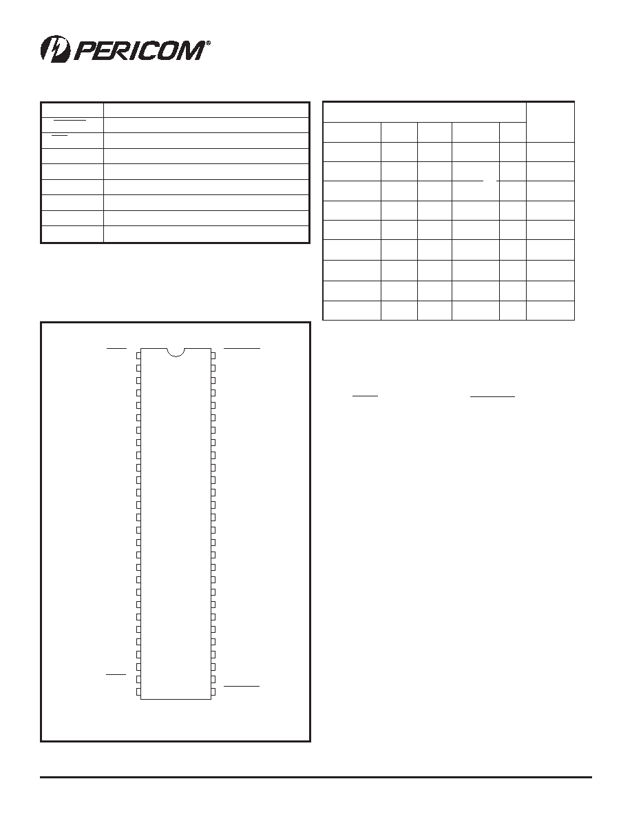
Product Pin Configuration
s
t
u
p
n
I
B
t
u
p
t
u
O
B
A
N
E
K
L
CB
A
E
OB
A
E
LB
A
K
L
CA
XH
X
Z
XL
H
X
L
XL
H
X
H
HL
L
X
B0 )
3
(
HL
L
X
B0 )
3
(
LL
L
↑
LL
L
↑
HH
LL
L
X
B0 )
3
(
LL
L
H
X
B0 )
4
(
OEAB
LEAB
A1
GND
A2
A3
VCC
A4
A5
A6
GND
A7
A8
A9
A10
A11
A12
GND
A13
A14
A15
VCC
A16
A17
GND
A18
OEBA
LEBA
CLKENAB
CLKAB
B1
GND
B2
B3
VCC
B4
B5
B6
GND
B7
B8
B9
B10
B11
B12
GND
B13
B14
B15
VCC
B16
B17
GND
B18
CLKBA
CLKENBA
06-0134
发布紧急采购,3分钟左右您将得到回复。
相关PDF资料
PI74ALVCH16260A
IC 12/14-BIT MUX/LATCH 56-TSSOP
PI74ALVCH16501A
IC UNIV BUS TXRX 16BIT 56TSSOP
PI74ALVCH16646A
IC TRANSCVR DUAL N-INV 56TSSOP
PI74ALVCH16652A
IC 16-BIT BUS TXCVR/REG 56-TSSOP
PI74ALVCH16721A
IC 20-BIT FLIP-FLOP 56-TSSOP
PI74ALVCH16823A
IC 18-BIT INTERFACE-F/F 56-TSSOP
PI74ALVCHR162245AEX
IC TXRX 16BIT BIDIR 3ST 48TSSOP
PI74ALVTC16241A
IC BUFF DVR TRI-ST 16BIT 48TSSOP
相关代理商/技术参数
PI74ALVCH162601V
制造商:未知厂家 制造商全称:未知厂家 功能描述:18-Bit Bus Transceiver
PI74ALVCH16260A
功能描述:IC 12/14-BIT MUX/LATCH 56-TSSOP RoHS:否 类别:集成电路 (IC) >> 逻辑 - 锁销 系列:74ALVCH 产品变化通告:Product Discontinuation 09/Dec/2010 标准包装:1,500 系列:74VCX 逻辑类型:D 型透明锁存器 电路:8:8 输出类型:三态 电源电压:1.8 V ~ 3.6 V 独立电路:2 延迟时间 - 传输:1.5ns 输出电流高,低:6mA,6mA 工作温度:-40°C ~ 85°C 安装类型:表面贴装 封装/外壳:48-TFSOP(0.240",6.10mm 宽) 供应商设备封装:48-TSSOP 包装:带卷 (TR)
PI74ALVCH16260A56
制造商:未知厂家 制造商全称:未知厂家 功能描述:Bus Exchanger
PI74ALVCH16260V
制造商:未知厂家 制造商全称:未知厂家 功能描述:Bus Exchanger
PI74ALVCH16260V56
制造商:未知厂家 制造商全称:未知厂家 功能描述:Bus Exchanger
PI74ALVCH16269
制造商:未知厂家 制造商全称:未知厂家 功能描述:Logic | 12/24-Bit Registered Bus Transceiver
PI74ALVCH16269A
制造商:Pericom Semiconductor Corporation 功能描述:Registered Bus Exchanger 1-Element 56-Pin TSSOP Tube 制造商:Pericom Semiconductor Corporation 功能描述:ALVC/VCX/A SERIES, 12-BIT EXCHANGER, TRUE OUTPUT, 56 Pin Plastic SMT
PI74ALVCH16269V
制造商:未知厂家 制造商全称:未知厂家 功能描述:Bus Exchanger